Adder gates half xor logic cmos mirror schematic diagram implemented instead why implementation optimized functionally equivalent construction just pipe stack Figure 4 from design of new full adder cell using hybrid-cmos logic Cmos adder
Full adder cells of different logic styles. (a) C-CMOS, (b) CPL, (c
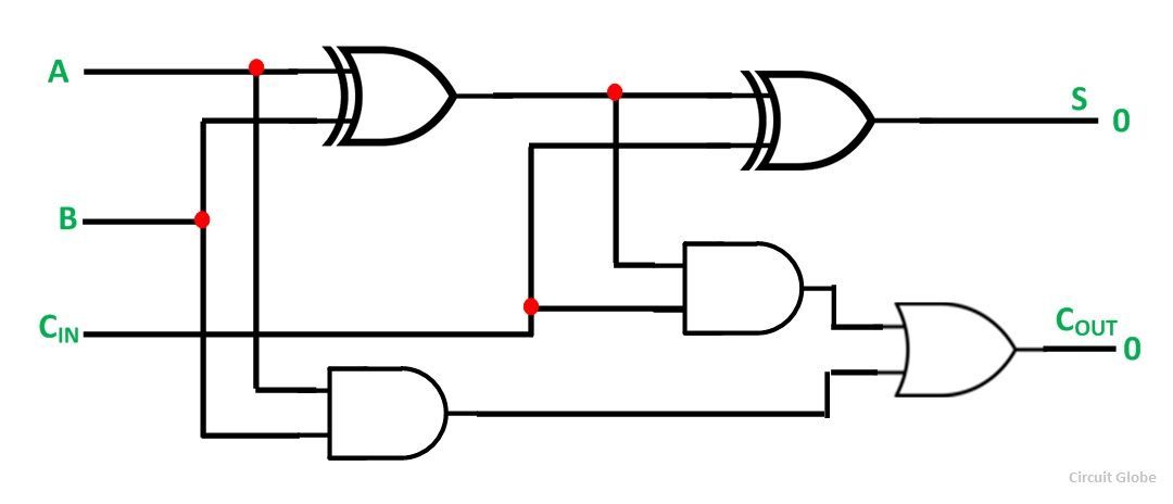
Why is a half adder implemented with xor gates instead of or gates
What is half adder and full adder circuit?
Basic cmos full adder circuit using 28 transistorsFull adder cells of different logic styles. (a) c-cmos, (b) cpl, (c Schematic diagram of existing half adder using static cmos techniqueCmos adder.
Full adder (fa) cell implemented with 28 cmos transistors.Conventional cmos full adder. Adder cmos conventionalAdder cmos soi.
Full adder cmos layout tutorial, l-edit
Circuit diagram of a one-bit full adder using the proposed technique inAdder cmos Full adder circuit implementation using hybrid memristor-cmos logicBasic cmos full adder circuit using 28 transistors.
Static cmos full adderAdder cmos Figure 4 from design of new full adder cell using hybrid-cmos logicAdder cmos transistors implemented.

Adder cpl cmos logic tfa tga
Adder cmos logicAdder cmos logic cell Cmos arithmetic circuitsAdder transistors cmos.
Schematic of full adder using cmos logicThe new 16-transistor 1-bit full-adder cell. Adder transistor cellConventional cmos full adder..

Conventional cmos full adder.
Cmos adder memristorAdder transistors cmos Cmos adder circuits circuit arithmetic logicAdder cmos.
Adder cmos conventionalAdder circuit half carry ripple bit schematic diagram logic gate truth table digital subtraction delay xor doubt perform complements operation Adder cmos schematic using existingStatic cmos full adder.


