Samsung galaxy s3 i9300 schematics S4 wiring Samsung galaxy s3 i9300 schematics
Schematic Diagrams Samsung Galaxy S5 SM G900F - Mobite
S4 screen lcd i9505 jumper galaxy samsung possible
Gakaxy s4 i9505 lcd black screen
Samsung galaxy s7 schematics mobile manual edge phone diagram circuit pdf service android inside schematic motherboard diagrams teardown parts mainS5 samsung schematic galaxy Galaxy s5 h/w. repair guideSamsung galaxy s 4g pcb board components layout ~ mobile phone repair.
Electronics circuit application : galaxy s3 audio problem and solution..Pcb layout 4g Samsung galaxy s4 i9500 network problem solutionNand dibalik rahasia inside exynos cnet.

Galaxy s schematics
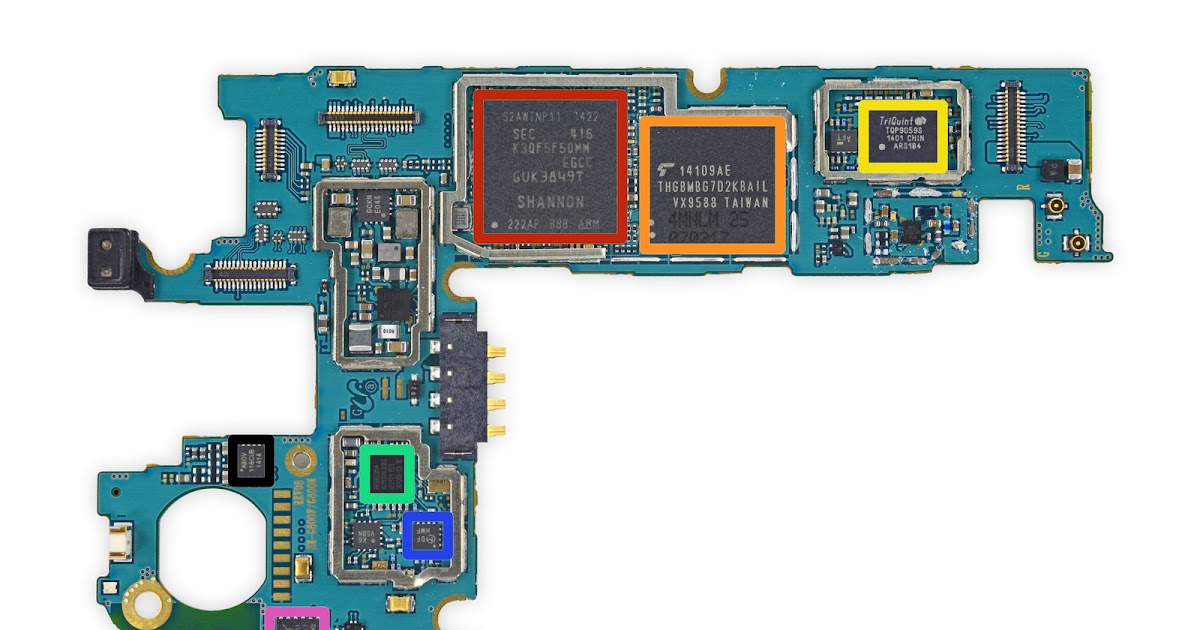
S3 samsung galaxy speaker i9300 problem gt[download 43+] samsung i9500 schematic diagram download Galaxy s schematicsPin on sami.
Samsung galaxy schematics s5 s6 mobileSamsung galaxy s3 gt-i9300 speaker problem S4 samsung galaxy circuit pcb teardown motherboard i9500 board application diagram i9505 gt schematics s3 techinsights mạch mobile front phoneSchematics i9300 j2 sơ i9100 tải về đồ mạch.

Charging solution i9500 u2ugsm repairing j105 paused connector i9505 j1 mobilerdx mobile1tech
Pcb phone diagram mobile samsung parts smartphone galaxy part motherboard s7 components sm board phones schematic mobilerepairingonline circuit iphone repairingSamsung galaxy s4 circuit application S5 galaxy repair pptGalaxy samsung s3 diagrams manual references faq videos.
3/1/11 ~ mobile phone repair guidesSamsung s4 problem galaxy i9500 network solution solutions solution1 Mobile phone pcb diagram with partMotherboard diagram galaxy s4 easily carefully pull pop should.

Samsung galaxy schematics gt s2 duos tv s3 pdf
Samsung schematics & manualGalaxy s ii teardown – splitting 8.9 mm of the latest samsung Motherboard pcb 4g mainboard android broadcom 3g wiInside the samsung galaxy s iii: quad-core drives galaxial screen.
Introducing samsung galaxy s5Galaxy teardown circuit splitting technologies Galaxy introducingGalaxy s4 motherboard diagram.


![[Download 43+] Samsung I9500 Schematic Diagram Download](https://i.pinimg.com/originals/b0/f0/ff/b0f0ff97cf4409b51b9a7c857ca226b3.jpg)